Classification of Materials:
Conductor: It is a material which conducts electricity, the conductivity of conductor is very high and resistance is so low.
In conductor electrons are charge carriers, the resistance of conductor increases with increase in temp. Impurity decreases the conductivity of conductor, in energy band diagram of conductor the conduction band and valence band overlap each other so that the charge flow is easy and fast.

Example of conductors are: Copper (cu), Aluminum (Al), Silver (Ag), etc.
Application of conductors : In production of electric wires.
Insulator: A material which doesn't conduct electricity is called an insulator. The conductivity of insulator is very low and the resistance is so high.
There is no charge carrier and no effect of temperature because its resistance coefficient is zero.
(NOTE: Resistance coefficient: The resistance-change factor per degree Celsius of temperature change is called the temperature coefficient of resistance.)
There is no change by adding any impurity in insulator.
In insulator, the forbidden energy gap between conduction band and valance band is very high.
Example: Rubber, plastic, etc.
Application: Insulating layers of wires or coating.
But before knowing semi-conductor, you might be thinking what the hell is Covalent and Valence bond.. right? So let's go through the definitions of Covalent and valance bons.
In an energy band diagram, there are three things namely, defined below.
1. Valence bond: The range of energy possessed by valanced electrons is called valence band. Electrons in the outermost orbit of the atom are called valance electrons, in a normal atom valence band has the electron of highest energy.
2. Conduction band: The valence electrons are losely attatched to the nucleaus at ordinary temprature, some of the valence electrons get detached to become free, in this band the electrons can gain energy from external electric field these free electrons are responsible for flow of current so they are called conduction electrons and the range of energy possessed by conduction electron is known as conduction band.
3.Forbidden energy gap(Fermi level gap): In between the lowest level of conduction band and highest level of valence band there is a gap that can't be occupy by the electrons which is called forbidden energy gap or band gap. In order to pose an electron from valence band to the conduction band, external energy equal to the forbidden energy gap must be supplied. In the image below the forbidden energy gap is represented by "Band Gap".


Conductor: It is a material which conducts electricity, the conductivity of conductor is very high and resistance is so low.
In conductor electrons are charge carriers, the resistance of conductor increases with increase in temp. Impurity decreases the conductivity of conductor, in energy band diagram of conductor the conduction band and valence band overlap each other so that the charge flow is easy and fast.

Application of conductors : In production of electric wires.
Insulator: A material which doesn't conduct electricity is called an insulator. The conductivity of insulator is very low and the resistance is so high.
There is no charge carrier and no effect of temperature because its resistance coefficient is zero.
(NOTE: Resistance coefficient: The resistance-change factor per degree Celsius of temperature change is called the temperature coefficient of resistance.)
There is no change by adding any impurity in insulator.
In insulator, the forbidden energy gap between conduction band and valance band is very high.
Example: Rubber, plastic, etc.
Application: Insulating layers of wires or coating.
But before knowing semi-conductor, you might be thinking what the hell is Covalent and Valence bond.. right? So let's go through the definitions of Covalent and valance bons.
In an energy band diagram, there are three things namely, defined below.
1. Valence bond: The range of energy possessed by valanced electrons is called valence band. Electrons in the outermost orbit of the atom are called valance electrons, in a normal atom valence band has the electron of highest energy.
2. Conduction band: The valence electrons are losely attatched to the nucleaus at ordinary temprature, some of the valence electrons get detached to become free, in this band the electrons can gain energy from external electric field these free electrons are responsible for flow of current so they are called conduction electrons and the range of energy possessed by conduction electron is known as conduction band.
3.Forbidden energy gap(Fermi level gap): In between the lowest level of conduction band and highest level of valence band there is a gap that can't be occupy by the electrons which is called forbidden energy gap or band gap. In order to pose an electron from valence band to the conduction band, external energy equal to the forbidden energy gap must be supplied. In the image below the forbidden energy gap is represented by "Band Gap".

Semi-Conductor: It is a material whose property lies between insulator and conductor (conductivity and resistance).
*In semi conductor the electrons and holes are charge carriers (Electrons for -ve and holes for +ve)
*The resistance of semi conductor decreases with rise in temperature.
*Impurity increases the electric conductivity of semi conductor.
*Conduction band and valence band are separated by very small forbidden energy gap of about 1 eV (electro-volt).

Example: Silicon and germanium.
Application: Semiconductor devices, etc.
As we're focusing on the topic "Semi-conductor"so let's go in detail about them.
Types of Semiconductor:
1. Intrinsic Semiconductor (Pure Semiconductor): In these types of semi conductors the electrical conductivity is totally governed by no. of electrons excited from valence band to conduction band.
example of intrinsic semiconductors are silicon and germaniam.
Both silicon and Ge have four electrons in the outermost shell which are called valence electrons. The four valence electrons form four covalent bonds with adjacent Si or Ge atom.
At absolute 0 temperature all the valence electrons are tightly bound to each Si atom there is no free electron is available for conduction so an intrisic semi conductor (Semi-C) behaves as insulator at absolute 0 temp. but at room temp. (25 - 27 degree celcius) or (300 kelvin) the energy of electron become so sufficient and covalent bonds get broken and the electrons become free they now move to the conduction band.
*The place where electrons are not present is called hole. the hole is considered as an active particle of valence band.
*In an intrinsic semi-C the total no. of electrons are equal to the total no. of holes.
*Below, the image shows electric conduction in intrinsic semiconductor:

2. Extrinsic Semiconductor: When a small quantity of pentavalent or trivalent impurity is introduced into pure semi conductor (intrinsic semi-c) its electrical conductivity increases and they become extrinsic semiconductors or impure semiconductors.
Doping: It is the process of adding impurity to an intrinsic semiconductor.
According to impurity added in pure semi-c it gets divided into two categories.
(i) N-type semi conductor: When a small quantity of pentavalent impurity such as antimony or arscenic is added to a pure semi conductor than the large no. of free electron are generated and this type of semi-conductor becomes N-type semi-c.

(ii) P-Type Semi-conductor: When a small quantity of trivalent impurity like boron or indium is added to pure semi conductor then the large no. of holes are generated, such type of semi-c is called p-type semi-c. In P-type semi conductor Holes are major charge carriers and Electrons are minor charge carriers.
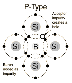
Note: Don't get confused in types of impurity, remember it with this trick- "P for N & T for P" (Pentavelant for N-type & Trivalent for P-type).
No comments:
Post a Comment